Tracking FOUPs in semiconductor manufacturing is important for contamination control, process optimization, yield improvement, quality control and compliance. It ensures the protection of wafers, optimizes workflow, enhances yield and maintains quality.
Application: FOUP traceability
Efficiently tracking FOUPs in semiconductor manufacturing can be challenging due to the complexity of managing numerous FOUPs, handling large amounts of data, integrating with existing systems, ensuring automation accuracy, dealing with environmental factors, and complying with industry standards.
Our solution: RFID for full process traceability
OMRON's RFID technology offers specialized features for semiconductor applications, including chemical resistance, compatibility with standardized glass transponders from Texas Instruments (reading and writing), and support for SECS I/II protocol.
This advanced solution supports five SEMI standards and SECS/GEM, ensuring consistent handling of FOUPs and pods in semiconductor fabs. Tailored for SEMI, this technology enhances wafer protection, optimizes workflow, and boosts yield and quality.
Enabling Technologies
V640 SEMI
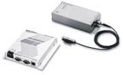
Semiconductor applications require special product features in terms of chemical resistance and protocol for identification systems. OMRON's V640 is able to provide both e.g. communication with standardized glass transponders from Texas Instruments and SECS I/II protocol as well.
Related Products

RFID system for use in various Semiconductor applications (FOUPS & pods)
Semiconductor applications require special product features in terms of chemical resistance and protocol for Identification systems. Omron's V640 is able to provide both e.g. communication with standardized glass transponders from Texas Instruments and SECS I/II protocol as well.
Do you want to know more?
Contact Our Experts
Contact Our Experts Wafer FOUP Traceability

Thank you for submitting your request. We will come back to you as soon as possible.
We are experiencing technical difficulties. Your form submission has not been successful. Please accept our apologies and try again later. Details: [details]